

A semiconductor is a material whose electrical conductivity sits between that of a conductor and an insulator — and, crucially, can be controlled. Copper wires conduct easily, rubber insulation barely conducts at all, but a semiconductor such as silicon can be switched from nearly insulating to highly conducting by adding tiny amounts of impurity, applying heat or light, or applying an electric field. That controllability is the reason semiconductors are the foundation of all modern electronics, from the simplest diode to the billions of transistors inside a computer processor.
Almost every electronic device you use depends on semiconductors: phones, computers, LED lights, solar panels, electric-vehicle power systems, and industrial motor drives. Understanding what a semiconductor is — and how doping turns a dull gray crystal into the most useful material in engineering — is the first step to understanding diodes, transistors, and integrated circuits.
Semiconductor Definition and Meaning
A semiconductor is a solid material with an electrical conductivity between a conductor (about 107 siemens per meter for copper) and an insulator (about 10−12 siemens per meter for glass). In its pure form, silicon — the most important semiconductor — is a poor conductor at room temperature. Only a small number of its electrons have enough thermal energy to break free from their atoms and carry current.
The word itself tells the story: “semi” means half, and “conductor” means a material that carries electric current. A semiconductor conducts partly, and — unlike a fixed resistor — its conductivity changes with temperature, light, and the impurities deliberately added to it. That sensitivity is not a weakness. It is exactly what engineers exploit to build devices that switch, amplify, sense, and convert energy.
The most common semiconductor materials are silicon (Si) and germanium (Ge), both group IV elements of the periodic table with four valence electrons. Compound semiconductors such as gallium arsenide (GaAs), silicon carbide (SiC), and gallium nitride (GaN) are used where silicon reaches its limits — in high-frequency radios, high-power converters, and bright LEDs.
Energy Bands and the Band Gap
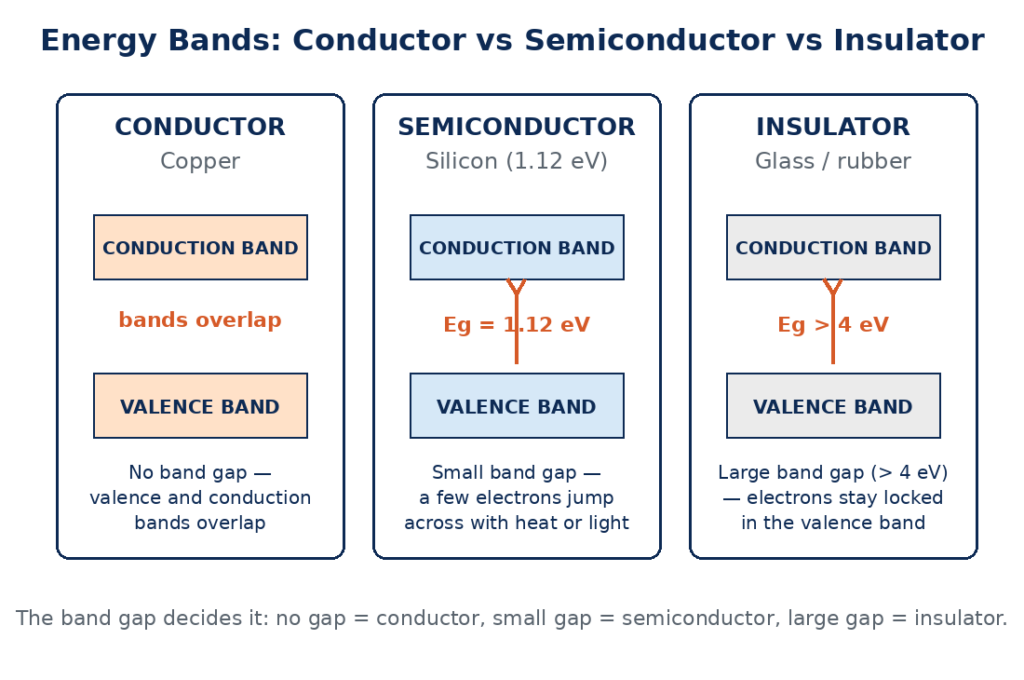
To understand semiconductors, picture the electrons in a solid as living in energy bands. The valence band holds the electrons bound to their atoms, and the conduction band holds the free electrons that can move and carry current. Between them lies the band gap — a forbidden range of energies where no electron can exist.
In a conductor such as copper, the valence and conduction bands overlap, so electrons move freely and current flows easily. In an insulator such as glass, the band gap is huge — more than 4 electron-volts (eV) — so almost no electron can jump across it, and current cannot flow. A semiconductor sits in between: its band gap is small, typically 0.1 to 3 eV. At room temperature, thermal energy pushes a small number of electrons across the gap, so a little current can flow — and any extra energy, from heat, light, or an applied voltage, pushes more electrons across.
Silicon has a band gap of 1.12 eV at room temperature, and germanium has a band gap of 0.67 eV. That difference matters: germanium leaks more current at high temperature, which is one reason silicon won the race and became the material of the entire electronics industry. Silicon is also abundant — it is the second most common element in the Earth’s crust — and it forms a stable, excellent insulating oxide (silicon dioxide) that makes chip manufacturing practical.
Intrinsic vs Extrinsic Semiconductors
Semiconductors come in two basic forms: intrinsic (pure) and extrinsic (doped). The difference between them is the difference between a raw material and an engineered one.
An intrinsic semiconductor is a chemically pure crystal — silicon or germanium with no intentional impurities. Its charge carriers come only from thermal excitation: each electron promoted to the conduction band leaves behind a hole in the valence band, so the number of electrons equals the number of holes (n = p). At room temperature, pure silicon has only about 1.5 × 10¹⁰ free carriers per cubic centimeter — far too few for practical devices, which is why pure silicon is rarely used on its own.
An extrinsic semiconductor is made by doping — deliberately adding a tiny amount of impurity atoms, typically a few parts per million, to the pure crystal. Doping changes the conductivity by orders of magnitude and creates two distinct types of material:
- N-type: doped with donor atoms from group V of the periodic table, such as phosphorus or arsenic. Each donor atom has five valence electrons, so it contributes one extra free electron. Electrons are the majority carriers, and the Fermi level shifts toward the conduction band.
- P-type: doped with acceptor atoms from group III, such as boron or gallium. Each acceptor atom has only three valence electrons, so it creates a hole — a missing electron that behaves like a positive charge carrier. Holes are the majority carriers, and the Fermi level shifts toward the valence band.
One fact surprises beginners: both N-type and P-type materials are electrically neutral overall. The extra electrons in N-type silicon are balanced by positively charged donor ions locked in the crystal, and the extra holes in P-type silicon are balanced by negatively charged acceptor ions. The letters N and P describe which carrier dominates, not a net electric charge.

How Doping Works: Donors and Acceptors
Doping works because silicon has four valence electrons and forms four covalent bonds with its neighbors in the crystal. Replace one silicon atom with a phosphorus atom, which has five valence electrons, and four of those electrons join the bonds while the fifth is only loosely held. A tiny amount of thermal energy frees it into the conduction band, where it can carry current. That is a donor atom: it donates a free electron.
Replace a silicon atom with a boron atom instead, and the opposite happens. Boron has three valence electrons, so one bond is left incomplete — a hole. A neighboring electron can hop into that hole, which moves the hole to the neighbor’s place. The hole drifts through the crystal as if it were a positive particle. That is an acceptor atom: it accepts an electron and creates a mobile hole.
The doping level controls the conductivity precisely. Adding just one impurity atom per million silicon atoms can raise the conductivity by a factor of a thousand or more. Chip manufacturers control doping to parts per billion, which is why a modern processor — with billions of transistors, each only a few nanometers across — can be manufactured reliably at all.
Common Semiconductor Materials
Silicon dominates, but it is not the only semiconductor in use. Each material’s band gap suits it to different jobs, as the table shows.
| Material | Band gap (eV) | Main uses |
|---|---|---|
| Germanium (Ge) | 0.67 | Early transistors, infrared optics, fiber optics |
| Silicon (Si) | 1.12 | Almost all chips, diodes, solar cells |
| Gallium arsenide (GaAs) | 1.43 | High-frequency radios, lasers, satellite electronics |
| Silicon carbide (SiC) | 3.26 | Electric-vehicle inverters, high-power, high-temperature use |
| Gallium nitride (GaN) | 3.40 | Fast chargers, 5G amplifiers, LED lighting |
| Diamond (C) | 5.47 | Extreme environments, experimental high-power devices |
Wide-band-gap materials such as silicon carbide and gallium nitride are the fastest-growing part of the field. Their larger band gaps let them switch higher voltages, run hotter, and switch faster than silicon — which is why SiC inverters now appear in electric cars and GaN chargers are smaller and cooler than the silicon chargers they replace.

The P-N Junction: Where Devices Begin
Join a piece of P-type material to a piece of N-type material and you get a P-N junction — the building block of nearly every semiconductor device. At the junction, electrons from the N side diffuse into the P side and holes diffuse the other way, until a thin depletion region forms with no free carriers. That region acts as a barrier that current can cross easily in one direction and barely at all in the other.
This one-way behavior is the working principle of the diode, which we explain in depth in our article on what a diode is. Stack two junctions together and you get a transistor, which can switch and amplify. Combine thousands or billions of transistors on one chip and you get an integrated circuit. Every one of those devices starts with the same idea: control the carriers in a semiconductor, and you control the current.
Properties of Semiconductors
- Controllable conductivity: doping, temperature, light, and electric fields all change how well a semiconductor conducts.
- Negative temperature coefficient of resistance: unlike copper, whose resistance rises with temperature, a semiconductor’s resistance falls as it gets hotter, because heat frees more carriers.
- Two types of carriers: both electrons and holes carry current, and devices can use either or both.
- Light sensitivity: photons with energy above the band gap create electron-hole pairs, which is how solar cells and photodiodes work.
- Rectifying junctions: a P-N junction conducts in one direction only, enabling diodes, rectifiers, and solar cells.
Applications of Semiconductors
Semiconductors are so widespread that listing every use would fill a book, but the main families are easy to group. In computing and communications, they form the processors, memory chips, and radio circuits in every phone, computer, and network device. In power electronics, diodes and transistors built from semiconductors rectify AC to DC, switch motor drives, and control the chargers and inverters in electric vehicles — see our guide to rectifier circuits for a classic example.
In sensing and light, photodiodes detect light, LEDs produce it, and thermistors and Hall sensors measure temperature and magnetic fields. In energy, silicon solar cells convert sunlight directly into electricity, and the global solar industry now installs hundreds of gigawatts of semiconductor-based panels every year. In industry, semiconductor devices drive automation, variable-speed drives, welding equipment, and uninterruptible power supplies.
Frequently Asked Questions
What is a semiconductor in simple words?
A semiconductor is a material, usually silicon, that conducts electricity partly — better than an insulator but worse than a metal — and whose conductivity can be controlled by adding impurities, heat, or light. That control is what makes diodes, transistors, and computer chips possible.
Is silicon a semiconductor?
Yes. Silicon is the most widely used semiconductor in the world. It has a band gap of 1.12 eV, it is abundant and cheap, and it forms a high-quality insulating oxide that makes chip manufacturing practical.
What is the difference between intrinsic and extrinsic semiconductors?
An intrinsic semiconductor is a pure crystal whose carriers come only from heat, with equal numbers of electrons and holes. An extrinsic semiconductor is deliberately doped with impurity atoms: donor doping makes N-type material (electrons dominate) and acceptor doping makes P-type material (holes dominate). Doping raises the conductivity by orders of magnitude.
Why is doping important?
Doping lets engineers set the type and concentration of charge carriers precisely. Without doping, silicon would be too poor a conductor for practical devices, and there would be no P-N junctions — no diodes, no transistors, and no integrated circuits.
What is the band gap of silicon?
Silicon’s band gap is 1.12 electron-volts (eV) at room temperature. Germanium’s is 0.67 eV and gallium arsenide’s is 1.43 eV. A larger band gap generally means the material can work at higher temperatures and voltages.
Conclusion
A semiconductor is a material whose conductivity can be engineered — and that single property built the modern world. Pure silicon barely conducts, but add a few parts per million of phosphorus or boron and you get N-type and P-type material whose carriers you can control. Join them into a P-N junction and you have a diode; add a second junction and you have a transistor; pack billions of transistors onto one chip and you have a computer. From solar panels to electric cars to the phone in your pocket, every major electrical technology of the last seventy years runs on semiconductors, and silicon — with its 1.12 eV band gap — remains the material that makes it all practical.
For a deeper look at how pure and doped silicon compare, including intrinsic carrier concentration and Fermi-level behavior, see the detailed reference at Electrical4U’s guide to intrinsic and extrinsic silicon.